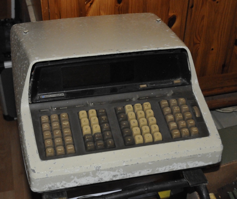
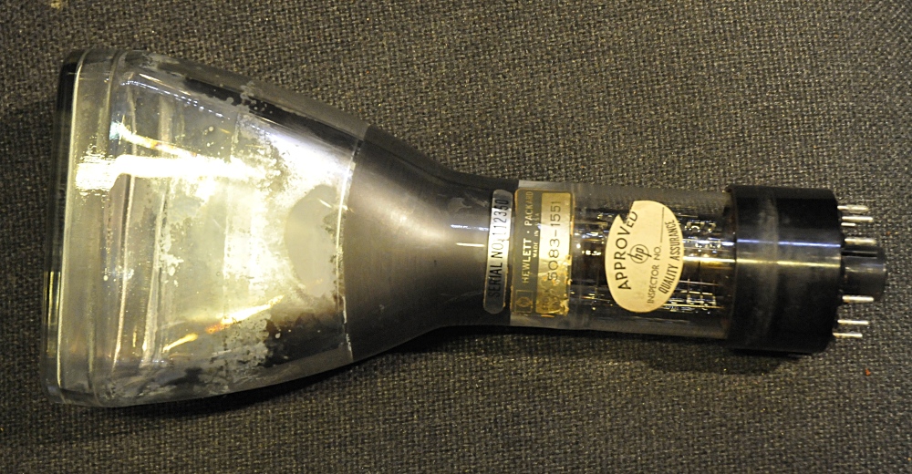
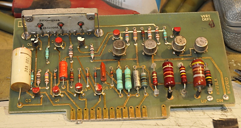
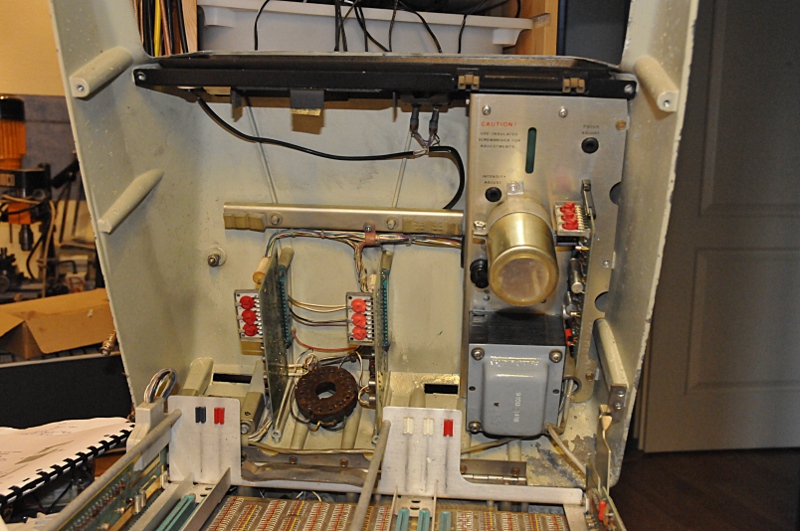
This is a report of progress made for the owner during the repair of a HP-9100B calculator. There are no microprocessors in side. It is one of the most famous calculators ever made. The first scientific calculator. I have no clue if it will succeed. It is in unknown and very bad condition. A thing that bothers me is a white spot in the CRT. Probably broken/leaking. A CRT ? Yes this uses a CRT to display results.
This calculator is not from me. I try to repair it for the HP calculator museum. http://www.calculatormuseum.nl/calc/
The calculator was once used by the Anthonie van Leeuwenhoek hospital and the person who had it from there, stored it under the floor in his house in Rotterdam, a few hundred meters from sea. (for the not-dutch, I live in the Netherlands most of our country is below the sealevel. The groundwater level is high on many places) So a lot of saltwater damage.
If you are looking for a 9100 to restore, be careful, this is a very complicated calculator. Most seem to have broken CRT’s. This is very hard to see because there is a metal shield around the CRT base. And that is the place they break. Good replacement CRT’s are very rare. There is no official service documentation, it is all lost (as far as I know at this moment). The design history of the 9100 is very interesting. A lot of anecdotes.
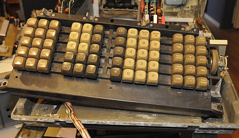
First step is cleaning the keyboard.
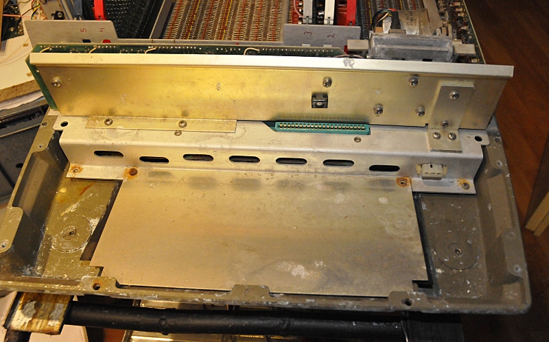
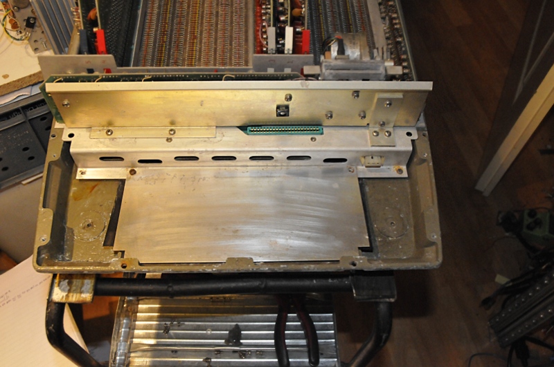
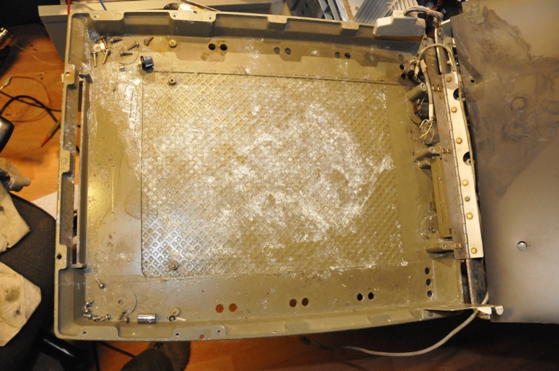
The white stuff is aluminum oxide, there was lots of it. You also see rust. Only two screws are in place. The others look like they are disintegrated. Just some rusty remainders are left, it does not look like the heads broke off. The rust around the holes make me think they just rusted away (not that strange because steel, water and aluminium together is not a good combination) The aluminium plate was very rough, hard to see on the picture, but it was very dirty
All cleaned up and shiny
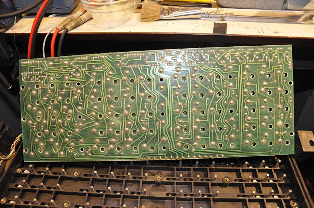
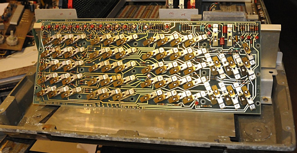
I make many pictures during a repair. So I am sure not to mix up connections. To remove the pcb I had to desolder it. It had to be removed for cleaning because there was a lot of oxidation inside. A white powder formed bridges between components and between leads and pcb.
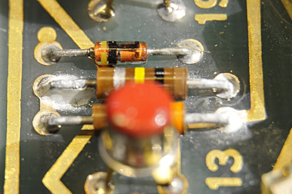
The bridge in the picture above was not forming a short but it was a nice example. Never seen something like this before.
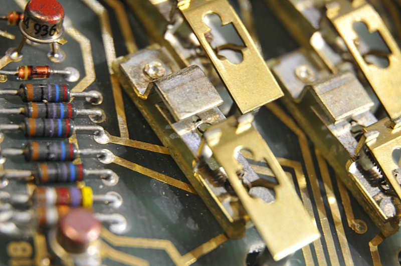
An uncleaned switch in the picture above. One switch was lose. You see the little spring that holds the floating contact against the L stud in the middle. This is connected to the gold color floating part. The bad thing is, the spring must be guided through a hole in that L-stud. Tip; fixate the switch contact between the Z shaped end, using a squeezed little plastic stick (like in the things you use to clean your ears)
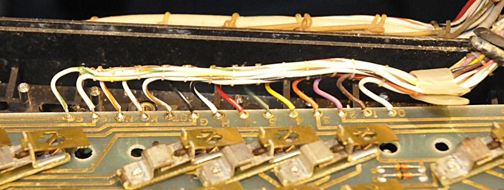
The pins you see sticking through the black plastic are from the keys. They actuate the switch contacts through holes in the board. There are small rubber rings on the pins. Most of them are missing. There function is damping the end of the keystroke travel.
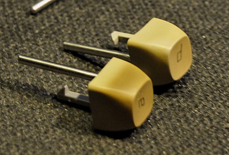
The keys were very dirty. First an ultrasonic bad and after that I polished them until they were nice again. Very boring and time consuming.
So I can see where to put the keys after cleaning.
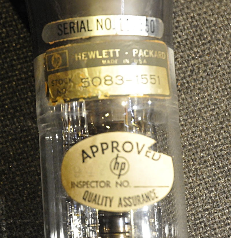
To bad the CRT is indeed dead. It is broken at the base.
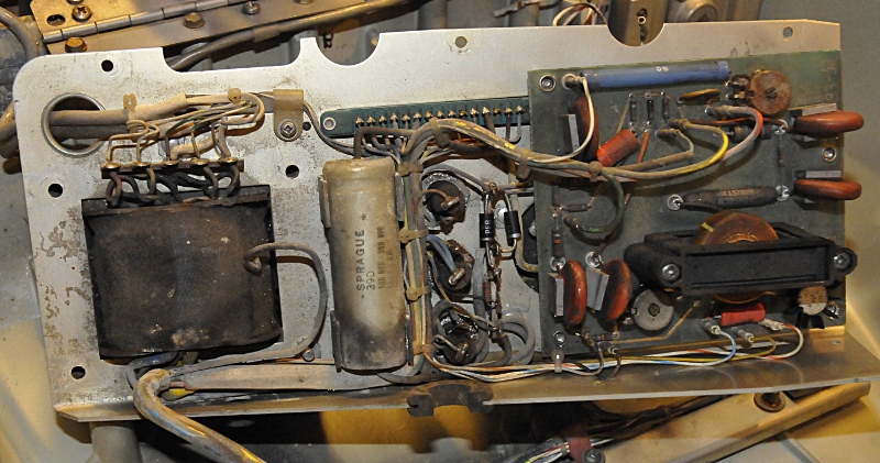
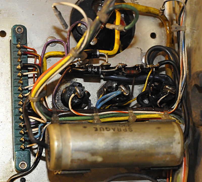
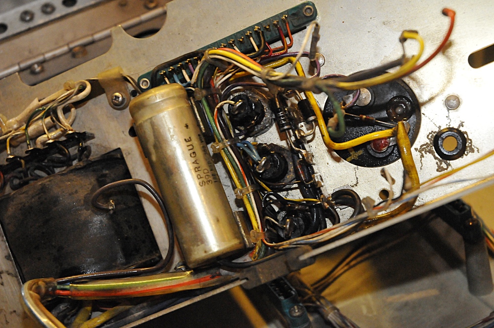
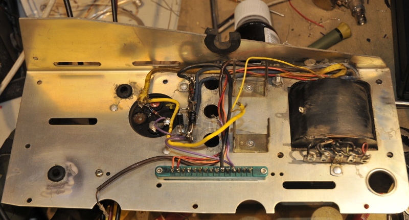
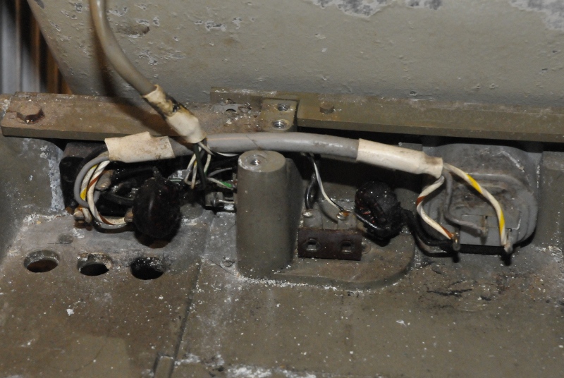
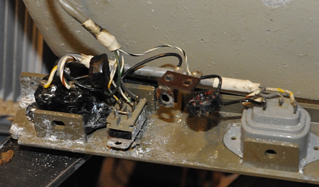
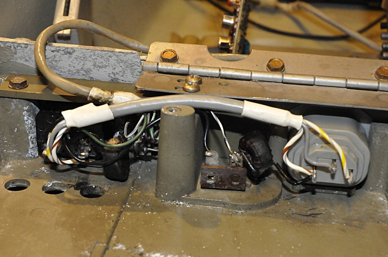
The PSU was a bit dirty and rusty.
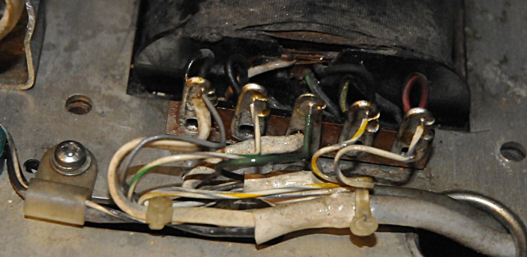
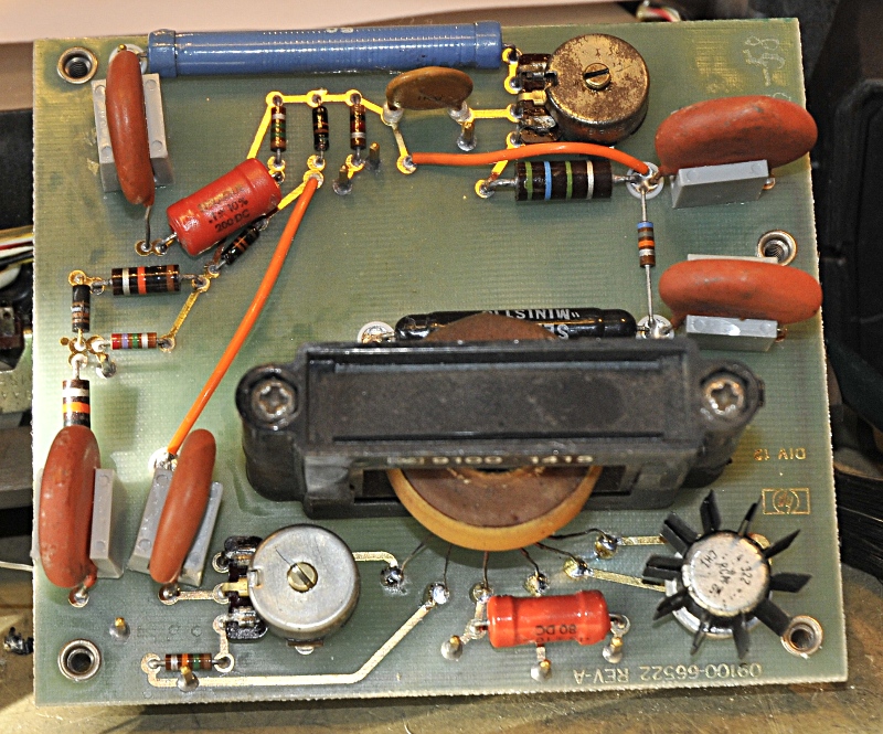
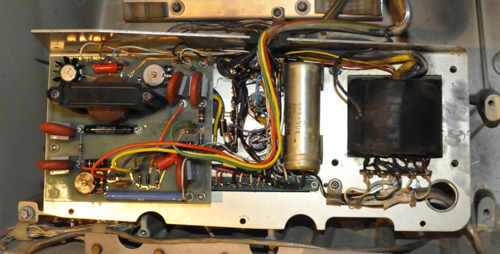
I removed all parts. The fuse holders were so rusty and dirty inside I had to remove them but to do that, I had to remove the PSU frame from the case and desolder all wires. The capacitor is fresh reformed, capacitance, D, ESR and leakage are perfect.
The rebuilded psu just before mounting:
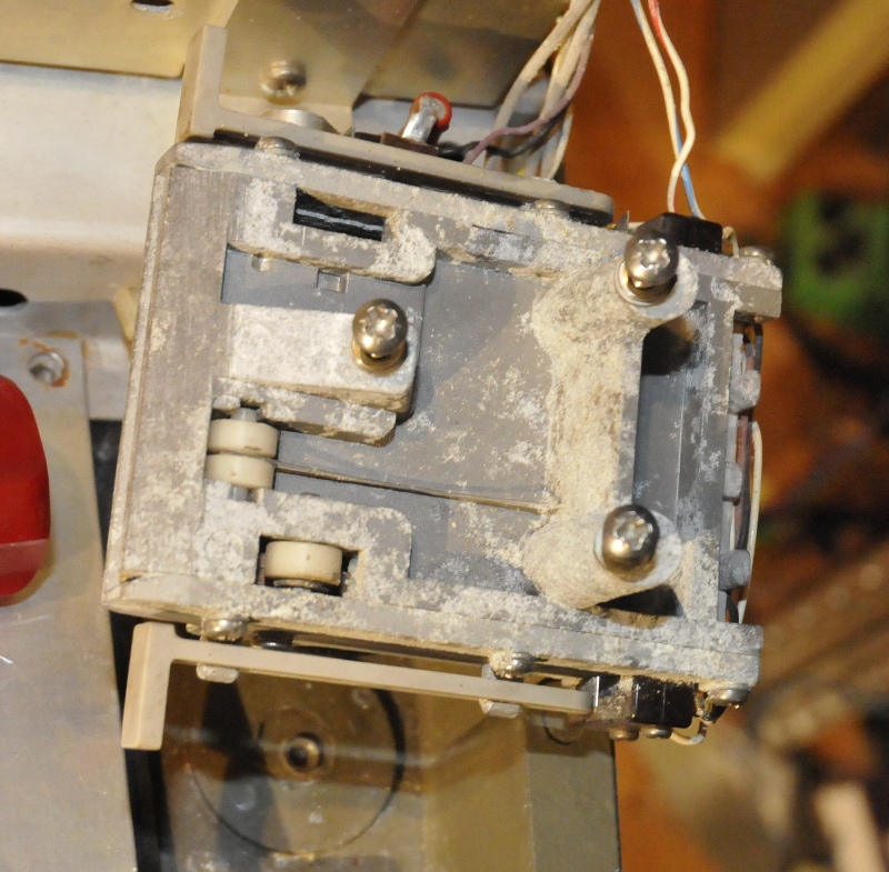
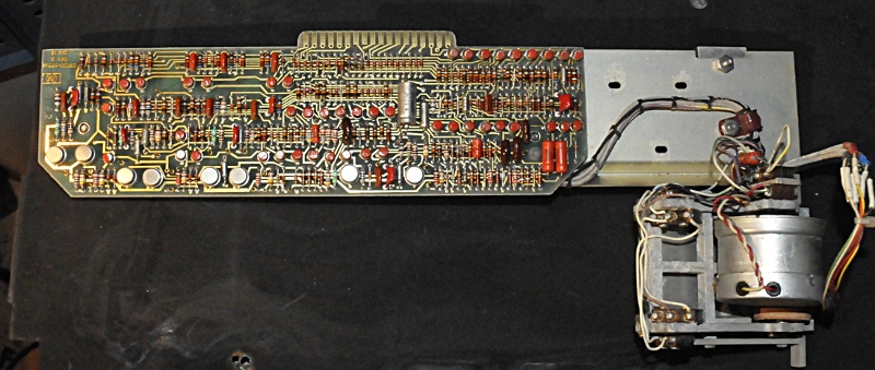
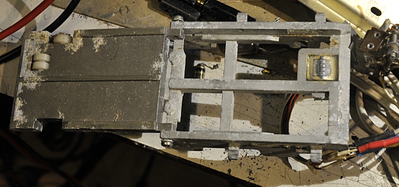
The cardreader is in real bad shape.
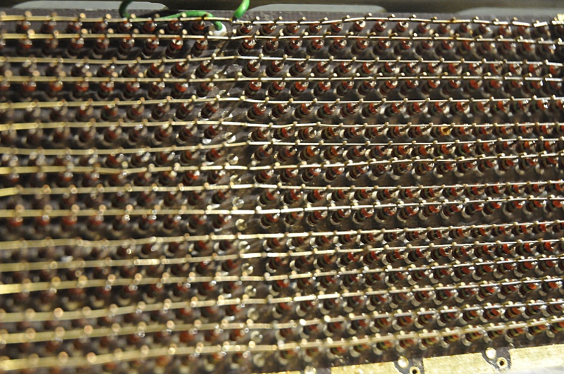
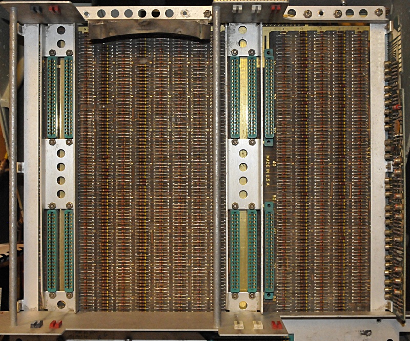
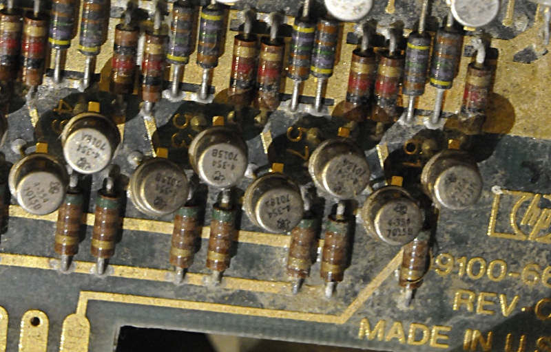
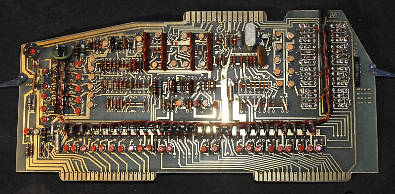
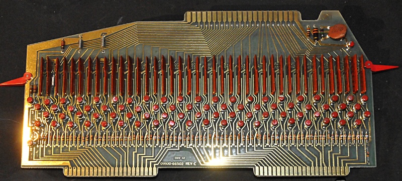
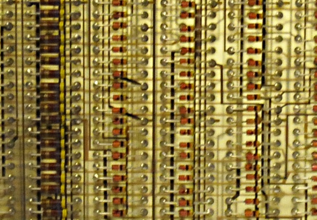
There are about 1800 diodes in the 9100B. 512 in the picture above. Besides this there are around 750 transistors and I guess around 2000 resistors.
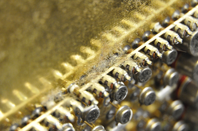
This picture above is not a out of focus in the middle. It is a web from a spider.
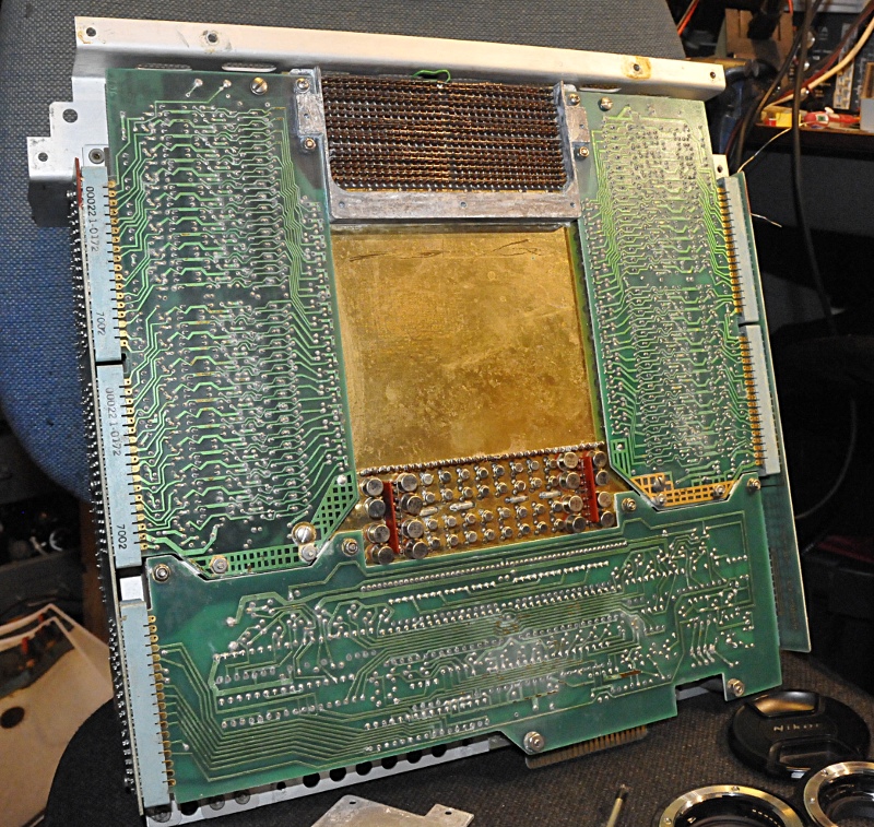
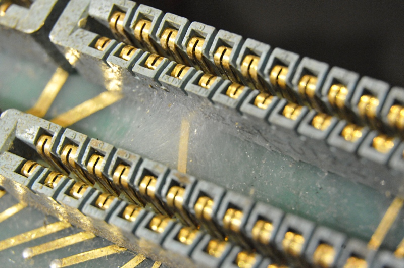
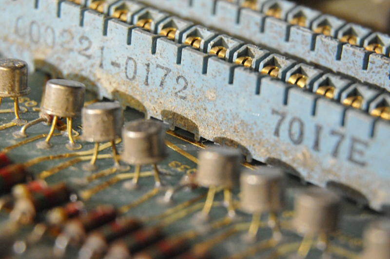
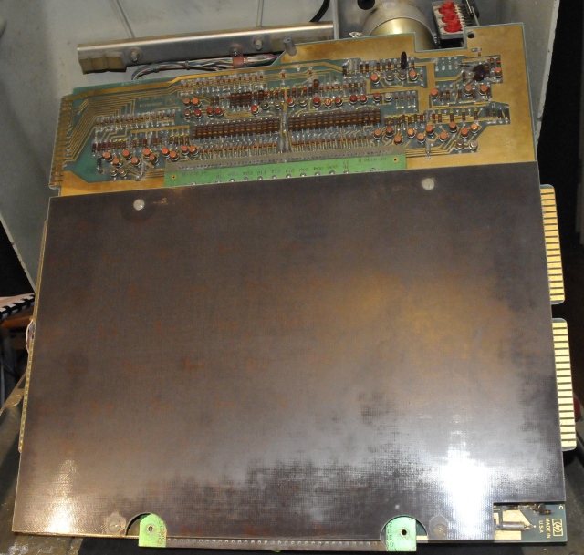
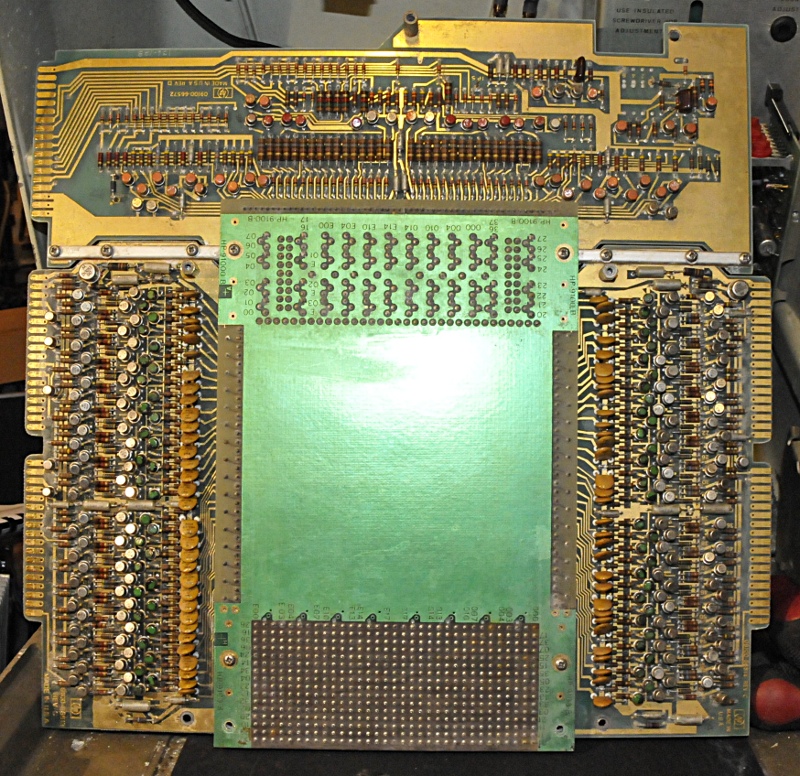
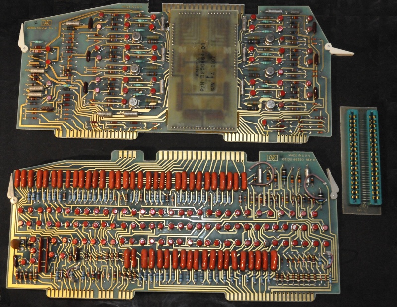
Top is the ROM adress decoder, left and right the ROM data control, the green (painted goldplated) board is the ROM. But not ROM as we know it. An inductive coupled multi-layer teflon construction. All the boards plugged on the RD board form a 64 bit processor !!!!. HP was the first to use Teflon for a pcb, at that time a new material. They were forced to find an alternative for the “normal” pcb materials because they could not get it to work.
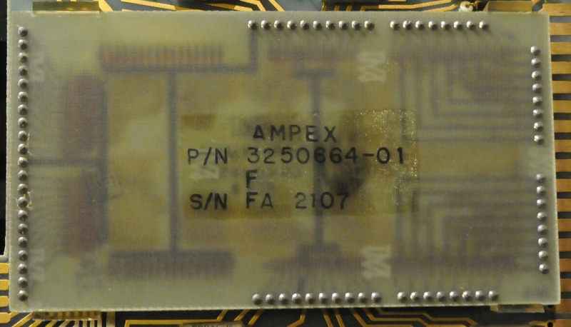
In 1968 the multilayer board above, was state of the art PCB building. Almost science fiction
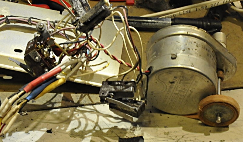
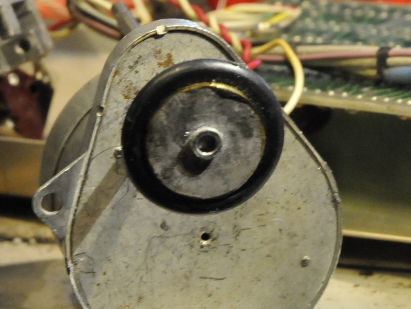
The wheel that transports the card is weird. I can not imagine this to be original. It is made of tape. total 25,1mm diameter. But it was not sticking anymore. So I had to find a substitude:
I used a automotive O-ring that had just the right size, 25.1mm again.
Meanwhile thanks to Guido, a CO member, I have a CRT usable as replacement.
Update: I was not able to repair it. I think the “firmware” pcb was corrupt. I had it working with the replacement tube but the results of calculations and keystrokes made no sense. The results were also not repeatable, just random. I repaired a 9100A for the same owner after this one. I used the best parts of both calculators to get one of them 100% working. See: http://www.pa4tim.nl/?p=3964

